
NMOS and PMOS
| Component | Symbol |
|---|---|
| NMOS | 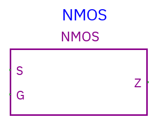 |
| PMOS | 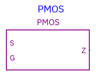 |
Both are digital pass devices: the gate signal controls whether source data reaches the output.
Pins: S source-data input, G control-data input, Z output. All pins have the configured width; multi-bit devices behave as parallel transistors. G is not necessarily a scalar enable bus.
| Component | Conducts when each G bit is | Disabled Z bit |
|---|---|---|
| NMOS | 1 | Z |
| PMOS | 0 | Z |
When conducting, each Z bit receives the corresponding S bit. Unknown G generally produces X, except a floating S remains Z. When disabled, the device releases the output; other drivers can still determine its shared net value.
Example NMOS: S=1, G=1 → Z=1; S=1, G=0 → Z=Z. PMOS has the opposite known control polarity.
Connect shared outputs with care: conflicting drivers produce X, and a released output allows another driver to determine the signal.