
Logic gates
AND, NAND, OR, NOR, XOR, XNOR
| Component | Symbol |
|---|---|
| AND | 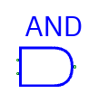 |
| NAND | 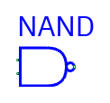 |
| OR | 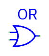 |
| NOR | 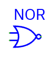 |
| XOR | 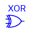 |
| XNOR | 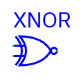 |
Pins: I0 … I<n−1> inputs, Z output. Configure input count (1–64) and
output/data width in Properties.
| Component | Operation on each bit | Scalar example |
|---|---|---|
| AND | All inputs must be 1 | 1 AND 0 = 0 |
| NAND | Inverted AND | 1 NAND 1 = 0 |
| OR | At least one input is 1 | 1 OR 0 = 1 |
| NOR | Inverted OR | 0 NOR 0 = 1 |
| XOR | Odd parity of inputs | 1 XOR 1 = 0 |
| XNOR | Inverted XOR | 1 XNOR 1 = 1 |
Buses are processed bit by bit. A single-bit logical input broadcasts across every bit of a wider gate: an AND gate with an 8-bit data input and a scalar enable of 1 passes the data; enable 0 produces zero.
A controlling input may determine the result even with unknowns: 0 AND X = 0,
1 OR X = 1. XOR with X/Z becomes X. Inverted variants invert the result, with
unknown remaining unknown.
Six reduction gates
| Component | Symbol |
|---|---|
| Reduction AND | 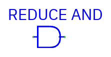 |
| Reduction NAND | 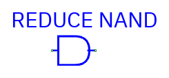 |
| Reduction OR | 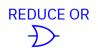 |
| Reduction NOR | 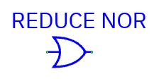 |
| Reduction XOR | 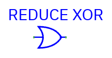 |
| Reduction XNOR | 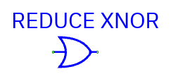 |
Entries: Reduction AND, Reduction NAND, Reduction OR, Reduction NOR, Reduction XOR, Reduction XNOR.
Pins: I0 is a bus input; Z is one bit, regardless of input width.
The width property is the input bus width. Default: eight input bits.
They apply their operation across all bits of that one bus:
- Reduction AND is 1 only if every bit is 1; NAND inverts it.
- Reduction OR is 1 if any bit is 1; NOR inverts it.
- Reduction XOR is 1 for odd population count; XNOR inverts it.
Example for I0 = 0x03 on eight bits: AND=0, NAND=1, OR=1, NOR=0, XOR=0,
XNOR=1.
Ordinary logic-gate Properties also has Reduce input bus to one bit. Disconnect before changing the reduction option because the pin width/layout changes. A dedicated reduction entry always remains a reduction gate.
Buffer and NOT
| Component | Symbol |
|---|---|
| Buffer | 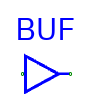 |
| NOT | 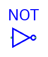 |
Pins: I input and Z output, matching data widths.
- Buffer produces the same known
0/1input. FloatingZor unknownXinput becomes X. - NOT inverts each known bit; X/Z becomes X.
Buffers preserve gate delay and isolate logic stages. Use Vdd/Ground or actual drivers rather than assuming an unconnected buffer input is zero.
Tri-state buffer
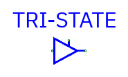
Pins: I data input, E one-bit enable, Z data output. Data width is
shared by I/Z. Properties contains Active-low enable and Invert enabled
output.
| Active-low | Invert | Verilog equivalent | Enabled at |
|---|---|---|---|
| Off | Off | bufif1 |
E=1 |
| On | Off | bufif0 |
E=0 |
| Off | On | notif1 |
E=1 |
| On | On | notif0 |
E=0 |
When disabled, Z is high impedance. Enabled inputs are buffered/inverted; enabled X/Z data becomes unknown. An unknown enable generally produces unknown output.
Several tri-state drivers can share a bus when only one drives it at once.
Conflicting active drivers produce X. An inverted tri-state gate is not
equivalent to an ordinary inverter after a tri-state gate: the separate inverter
turns a floating input into X, whereas a disabled notif output stays Z.
Typical use: register data → I, arbitration control → E, shared bus ← Z. Probe the bus to detect conflicts.